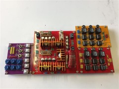
Jieduo state technologyPCB Assembly Manufacturer Printed circuit board design is based on the circuit schematic, to achieve the circuit designer needs. Printed circuit board design mainly refers to the layout design, need to consider the layout of external connections. Optimization of internal electronic components. Optimized layout of metal connections and vias. Electromagnetic protection. Heat dissipation and other factors. Excellent layout design can save production costs, achieve good circuit performance and thermal performance. Simple layout design can be done manually, and complex layout designs need to be implemented with computer aided design (CAD). In high-speed designs, the characteristic impedance of the controllable resistors and lines is one of the most important and common problems. First, look at the definition of the transmission line: the transmission line consists of two conductors with a certain length, one conductor used to send the signal, the other used to receive the signal (remember "loop" to replac the "ground" concept). In a multilayer board, each line is part of the transmission line, and the adjacent reference plane can be used as a second line or loop. The key to becoming a "good performance" transmission line is to keep its characteristic impedance constant throughout the line. [1] The key to making the board a "controllable impedance plate" is to make the characteristic impedance of all lines meet a specified value, usually between 25 ohms and 70 ohms. In multilayer circuit boards, the key to good transmission line performance is to keep its characteristic impedance constant across the entire line. But what exactly is the characteristic impedance? The easiest way to understand the characteristic impedance is to see what the signal is in the transmission. This is similar to the microwave transmission shown in Figure 1 when moving along a transmission line with the same cross-section. Assuming that a 1 volt voltage step wave is applied to this transmission line, such as a 1 volt battery connected to the front end of the transmission line (which is located between the transmission line and the circuit), once connected, the voltage wave signal along the line to the speed of light Spread, its speed is usually about 6 inches / nanosecond. Of course, this signal is indeed the voltage difference between the transmission line and the loop, which can be measured from any point of the transmission line and the adjacent point of the loop. Figure 2 is a schematic representation of the transmission of the voltage signal. Zen's method is to "generate a signal" and then spread along the transmission line at a speed of 6 inches / nanosecond. The first 0.01 nanosecond forward 0.06 inches, then send the line there are excess positive charge, and the circuit has excess negative charge, it is these two kinds of charge difference between the two conductors to maintain the voltage difference between 1 volt, And these two conductors and formed a capacitor. In the next 0.01 nanoseconds, it is necessary to adjust the voltage of a 0.06-inch transmission line from 0 to 1 volt, which must add some positive charge to the transmission line and add some negative charge to the receiving line. For each move of 0.06 inches, more positive charge must be added to the sending line, and more negative charge is added to the loop. Every 0.01 nanoseconds, the other part of the transmission line must be charged, and then the signal begins to propagate along this segment. The battery from the front end of the transmission line, when moving along this line, charges the continuous portion of the transmission line so that a voltage difference of 1 volt is formed between the transmission line and the circuit. A constant charge (± Q) from the battery is given a constant current (± Q) for a constant time interval (± t). The negative current flowing into the circuit is actually equal to the positive current flowing out, and at the front end of the signal wave, the AC current flows through the upper and lower lines to complete the entire cycle. is focused on Approved PCB Prototype Factory, PCB Online industry ranking, Durable PCB Online, Ascendant PCB Assembly Manufacturer and other projects. even though in the rapid development of the project ,Jieduo state technology always stressed the balance between external opportunities and internal management, attaches great importance to the core compet
Jieduo state technologyadheres to advance with the times and advocates to the service-oriented,faith-based, people-oriented management idea. With a belief of customer first to forge ahead , company insists on providing our clients with satisfying and best service ofelectronic PCB assembly,PCB SMTx19b655en,


