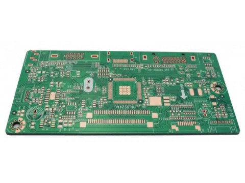
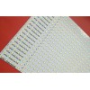
The multi-layer PCB has at least 3 layers of conductive layers, 2 of which are on the outer surface, and the remaining layer is synthesized in the insulation board. Multilayer PCB combines several single PCBs and double-sided PCBs together through insulating materials and positioning systems. It has multiple layers of wiring layer. Each layer is a medium layer, and the medium layer can be made very thin. The electrical connections between them are usually achieved through the plating holes on the horizontal surface of the circuit board.

Application:
With the rapid development of electronic information technology and the requirements of electronic products in the fields of medical, aviation, and computers, the circuit board has gradually developed in the direction of light quality, small volume, and density. Due to the limitation of space size by single and double-sided circuit boards, the possibility of further enhance the density of assembly density is getting smaller and smaller, so a multi-layer circuit board with higher assembly density and higher layers needs to be used. The multi-layer circuit board is widely used in the field of electronic products with its stable electrical performance, excellent economic performance, and design flexibility.

Advantages:
1. Light quality, smaller volume, and high assembly density, which can meet the diversified demand with light and small volume;
2. Good assembly, the connection of each component is reduced, the installation is relatively easy, and the reliability is relatively high;
3. The graphic has consistency and repetitiveness, reduces the error rate of assembly and wiring, and greatly shortens the time of maintenance and commissioning;
4. It can increase the number of wiring layers and increase design flexibility;
5. It can build a line with a certain impedance, which can form a high-speed transmission line
6. The metal core heat dissipation layer and magnetic circuit and line shielding layer can be set to meet the needs of heat dissipation and shielding.

Production Features:
1. Long-term reliability management
Development from general automotive PCBs to heavy-duty PCBs.
2. Rich experience in the manufacturing technology of multi-layer PCBs
Full-range industrial control equipment and communication PCBs
3. Full range products, small-medium-large batches, short delivery time
・Small, medium and big QTY (1PC~2000㎡/Lot)
・Multiple varieties (3000~5000 product names/month)
4. Short lead times (for small batches)
5. Surface treatment: OSP, lead-free HASL (Sn-Ag-Cu, Sn-Ni-Cu), immersion gold, electro-gold, immersion tin
PCB Delivery Date:

Manufacturing Process:
Copper clad plate cutting → Inner layer graphic production → Lamination → Drilling → Copper plating → Outer layer graphic production → Resistance welding → Text → Surface treatment → Appearance processing → Electrical inspection → Appearance inspection → Packaging → Shipping.

https://www.ronghuaindustry.com/multilayer-pcb
Email: sales@ronghuaindustry.com

