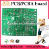
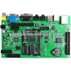
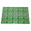
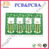
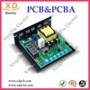
pcb for led

Click image to view original image
Price: Negotiable
Min.Order:
Supply
Delivery: Shipment within 3 days since the date of payment
Address: China
Valid until: Never Expire
Updated on: 2013-03-26 15:37
Hits: 1002780
Enquiry
Company Detail
 
 
Details


Detailed Product Description

Specifications 
1.Competitive price 
2.Prompt Reply& Delivery 
3.High quality, Best service 
4.ISO9001/TS16949/ROHS 

Specifications

LCD projector PCBA 
1.Competitive price 
2.Prompt Reply& Delivery 
3.High quality, Best service 
4ISO9001/TS16949/ROHS

          Welcome to XingDa Electric Technology Co., Ltd

                 Xindaxing Electric Technology Co., Ltd 

We are professional manufacturer in various PCB and PCBA for many years .We can provide a reasonable price with high quality products.

 XingDa who can provide a full set of service.such as below:

* 1. PCB layout, PCB design

* 2: Make high difficulty PCB (1 to 38 layers)

* 3: Provide all Electronic component

* 4: PCB assembly

* 5: Write programs for clients

* 6: PCBA/finished product Test. etc.

1.specification 


Item

Specification


1

Number of Layer

1-38Layers


2

Material

FR-4,FR2.Taconic,Rogers, CEM-1 CEM-3,ceramic , crockery Metal-backed Laminate,Aluminum etc.


3

Finish Board Thickness

0.2mm-6.00 mm(8mil-126mil)


4

Minimum Core Thickness

0.075mm(3mil)


5

Copper Thickness

1/2 oz min;12 oz max


6

Min. Trace Width & Line Spacing

0.075mm/0.1mm(3mil/4mil)


7

Min. Hole Diameter for CNC Drilling

0.1mm(4mil)


8

Min. Hole Diameter for punching

0.9mm(35mil)


9

Biggest panel size

610mm*508mm


10

Hole Position

+/-0.075mm(3mil) CNC Drilling


11

Conductor Width(W)

0.05mm(2mil)or;+/-20% of original artwork


12

Hole Diameter(H)

PTH L:+/-0.075mm(3mil);Non-PTH L:+/-0.05mm(2mil)


13

Outline Tolerance

0.125mm(5mil) CNC Routing;+/-0.15mm(6mil) by Punching


14

Warp & Twist

0.70%


15

Insulation Resistance

10Kohm-20Mohm


16

Conductivity

<50ohm


17

Test Voltage

10-300V


18

Panel Size

110×100mm(min);660×600mm(max)


19

Layer-layer misregistration

4 layers:0.15mm(6mil)max;6 layers:0.25mm(10mil)max


20

Min. spacing between hole edge to circuity pattern of an inner layer

0.25mm(10mil)


21

Min. spacing between board outline to circuitry pattern of an inner layer

0.25mm(10mil)


22

Board thickness tolerance

4 layers:+/-0.13mm(5mil);6 layers:+/-0.15mm(6mil)


2.Details for PCB Assembly

Technical

1).Professional surface mounting and through hole soldering technology;

2).Various sizes,like 1206,0805,0603 components SMT  technology;

3).ICT(In Circuit Test),FCT(Functional Circuit Test)  technology;

4).Nitrogen gas reflow soldering  technology for SMT;

5).High standard SMT&Solder Assembly line;

6).High density interconnected board placement technology capacity.

Quote requirement

1).The detailed files(Gerber files,specification and  BOM);

2).Clear pictures of PCBA or samples for us;

3).PCBA Test method. 

Total: 0 [Show All]  Related Reviews
 
More »Our Others Products

[ ProductsSearch ]  [ Add To Favourite ]  [ Tell Friends ]  [ Print Content ]  [ Violation Report ]  [ Close Window ]