


Detailed Product Descript ion
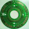
High Frequency PCB
1.PCB layout, PCB design
2.1 to 38 layers PCB
3.Provide all Electronic compocomponents
4. prompt deliery
Specifications
PCB electronic contract manufacturing
1.PCB Layout,PCB design
2. 1-38 layers PCB boards
3. UL, ROHS, T/S16949, ISO14000, ISO9001
4. Markets: worldwide
5. Timely delivery
PCB electronic contract manufacturing
1.PCB Layout,PCB design
2.Make high difficulty PCB(1-38 layers boards)
3.offer all Electric components
4.ISO9001/TS16949/ROHS
5.PCB delivery time:5-10 days; PCBA delivery time:20-25 days
Welcome to XingDa Electric Technology Co.,Ltd
Xindaxing Electric Technology Co.,LTd
We are professional manufacturer in various PCB and PCBA with many years experience,We can provide a reasonable price with high quality products.
XingDa who can provide a full set of service.such as below:
* 1. PCB layout, PCB design
* 2: Make high difficulty PCB(1 to 38 layers)
* 3: Provide all Electronic component
* 4: PCB assembly
* 5: Write programs for clients
* 6: PCBA/finished product Test. etc.
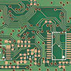
1.PCB Specification detail.
2.Details for PCB Assembly
Technical
1).Professional surface mounting and through hole soldering technology;
2).Various sizes,like 1206,0805,0603 components SMT technology;
3).ICT(In Circuit Test),FCT(Functional Circuit Test) technology;
4).Nitrogen gas reflow soldering technology for SMT;
5).High standard SMT&Solder Assembly line;
6).High density interconnected board placement technology capacity.
Quote requirement
1).The detailed files(Gerber files,specification and BOM);
2).Clear pictures of PCBA or samples for us;
3).PCBA Test method.